Full adder using half adder verilog code Solved which logic diagram is specified by the following Solved 5.28 the verilog code in figure p5.9 represents a
Draw the circuit corresponding to the Verilog module | Chegg.com
Schematic verilog circuit vhdl pyroelectro tutorials introduction full intro
Circuit diagram to verilog code
Draw the circuit corresponding to the verilog moduleSolution: verilog coding examples of digital circuits Solved 2. (a) write a verilog description of the circuitSolved a) write a verilog module for the circuit below using.
Verilog reset dff circuit module sync schematic synthesis modulesVerilog module Verilog transcribedSolved it is required to shown circuit using verilog without.

Solved draw the circuit corresponding to the verilog module
[diagram] mitsubishi m64 wiring diagramSolved a) write a verilog module for the circuit using An introduction to verilogCircuit diagram to verilog.
Full adder circuit diagram in verilogGetting started with the verilog hardware description language Solved 9. develop a verilog program for the block diagramSolved implement schematic circuit to verilog code.
Circuit diagram to verilog
Module circuit verilog write using structural style solvedCircuit diagram to verilog For the following verilog code, draw theGenerating automatic schematics from verilog/vhdl/system verilog.
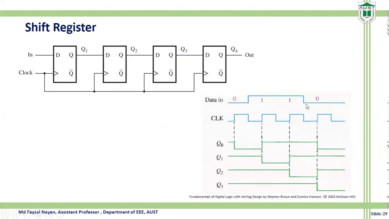
Verilog circuit chegg shown transcribed module delayFull adder circuit diagram in verilog Step 1: implement the circuit in verilog a ins inVerilog code shift register bit lfsr figure represents linear feedback solved draw p5 type input random reg circuit module number.
![[DIAGRAM] Mitsubishi M64 Wiring Diagram - MYDIAGRAM.ONLINE](https://i2.wp.com/i.stack.imgur.com/dEB5g.png)
Verilog circuit module code write below style using file separate structural turn create transcribed text show xy
Full adder verilog codeStep 1: implement the circuit in verilog a ins in Solved draw the equivalent circuit diagram and synthesizedSolved build the schematic circuit in verilog for the module.
Digital logic circuit design using verilogSolved 2. draw the circuit that this verilog segment Verilog hardware language description example started getting schematic articles figureSolved 16 (a) write a verilog module to describe the circuit.

Circuit diagram to structural verilog
Verilog vhdl schematics generating automatic system rtlDigital schematic and layout diagram .
.


